MAIN COMPETENCES
Research
Leadership
Teamwork & Communication
Volunteering & Social Service
Excel
Word
Power Point
Python
R
C++
MATLAB & Simulink
Web Development
Machine Learning
Deep Learning
Artificial Intelligence
Corporate Finance
Semiconductor Manufacturing
2D Materials Fabrication

Sajith

Withanage, Ph.D.

Materials Scientist | Condensed Matter and Materials Physicist | Expert 2D - Materials Grower | Former APS Student Ambassador for the Georgia State University

If your actions inspire others to dream more, learn more, do more & become more, YOU ARE A LEADER.”

– John Quincy Adams

“Coming together is a beginning, staying together is progress, and working together is success.” 

– Henry Ford

“Teamwork is the ability to work together toward a common vision. The ability to direct individual accomplishments toward organizational objectives. It is the fuel that allows common people to attain uncommon results.”

― Andrew Carnegie

The walk of success!

— Your limitation - it’s only your imagination —

GPA: 3.52    2016-2021

Research & Development

Publication Link | Download PDF | Cite This

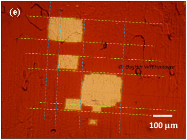
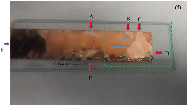
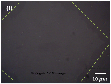
Abstract: Graphene has attracted enormous attention due to its unique characteristics. However, the LPCVD graphene grown on copper turns out to be polycrystalline because of the high nucleation density (ND) on the copper foil surface. In order to realize better quality LPCVD graphene, this ND needs to be significantly reduced. Based on the observations from our initial graphene growths on as-received copper, we figured that the uneven Cu surfaces with defects produce large NDs. At a large ND, the graphene flakes nucleated at different sites coalesced to produce polycrystalline graphene. Due to such issues, we have implemented an electropolishing technique to smoothen the native surface of the copper foil. We will discuss the successful implementation of the surface smoothening process to reduce nucleation site formation while limiting the surface defects (which leads to wrinkle formation). The annealing process was also helpful to flatten the surface during the growth process further. We have also observed that graphene grows across Cu grain boundaries and, in the process, produces an additional surface area for graphene growth. That later causes to form wrinkles, which affect graphene properties negatively.

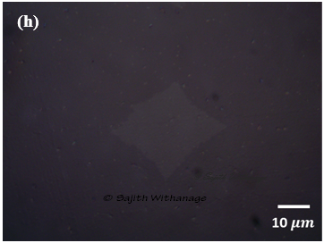
In the next project, the effect of multi-step copper surface oxidization, base pressure vacuum in the middle of the process, and integration of Cu enclosures on suppressing the ND will be discussed. The technique is based on the self-cleaning characteristics of copper oxides and the metal evaporation in a high vacuum at high temperatures. The ND has reduced to ~5 nucleation per square centimeter on average (an improvement compared to the previously reported minimum value, ten per square centimeter  which was obtained using copper enclosures), and the graphene/copper surface has become smoother. The self-aligned graphene island geometry and shape of the flakes have reflected the symmetry and the single crystallinity of graphene.

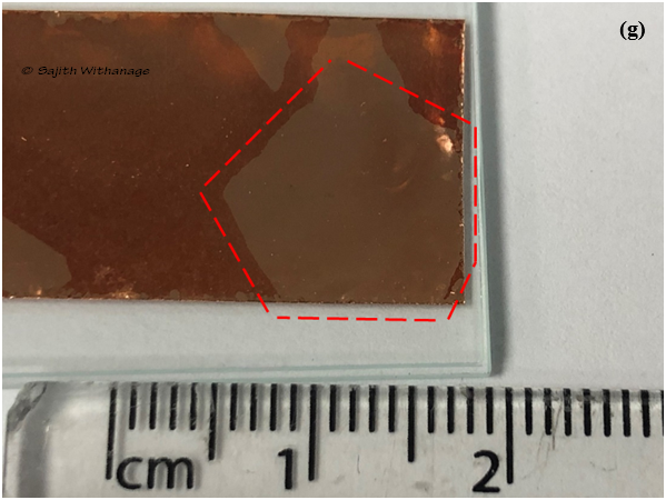
The final project will discuss the growth of cm-scale graphene flakes on Cu and 3D-multilayered graphene on 3D-Ni foams and used Ni’s gettering carbon diffusion effect to make the Cu foil carbon-free. The Ni-foam/Cu enclosure was oxidized in situ to assist with the self-cleaning process of metal oxides. The ND has been reduced to ~0.57 per square centimeter  and obtained cm-scale graphene flakes.

Publication Link | Cite This

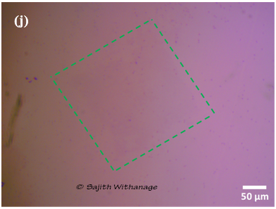
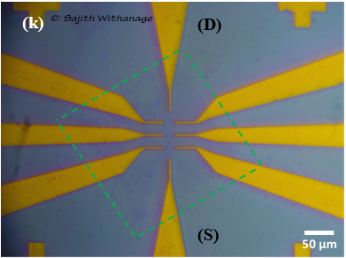
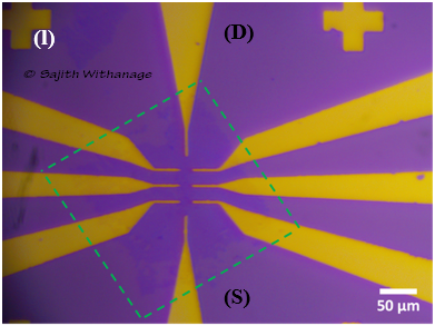
Abstract: There has been much recent interest in transferring 2D materials on to non-conducting surfaces. One approach was to pick-up graphene grown by the CVD method using a flake of hexagonal boron nitride (hBN) to have a contamination-free dry transfer. But this kind of transfer technique can be only used in small-scale device fabrication for laboratory use since the scale limitations of the hBN flakes and the limited supply of hBN flakes with low thicknesses. Here, we report a hybrid transfer technique that combines wet and dry transfer processes using polymer support resulting in wrinkle and contamination-free high mobility 2D materials. Thus, we detail the transfer process, conditions for a successful transfer and the quality of CVD grown graphene. The transferred graphene layers are characterized by various methods, and the results of the study are reported.

Publication Link | Download PDF | Cite This

Abstract: CVD graphene growth typically uses commercially available cold-rolled copper foils, which includes a rich topography with scratches, dents, pits, and peaks. The graphene grown on this topography, even after annealing the foil, tends to include and reflect these topographic features. Further, the transfer of such CVD graphene to a flat substrate using a polymer transfer method also introduces wrinkles. Here, we examine an electropolishing technique for reducing native foil defects, characterize the resulting foil surface, grow single-crystal graphene on the polished foil, and examine the quality of the graphene for such defects.

Publication Link | Download PDF 

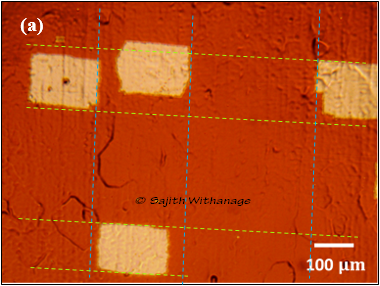
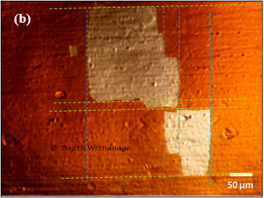
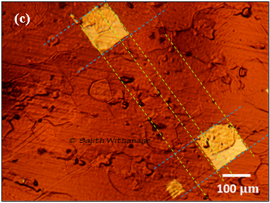
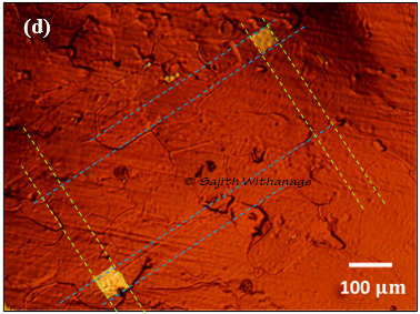
Abstract: The formation of wrinkles due to thermal expansion coefficient differences between the underlying substrate and 2-D materials during the cooling stage after high temperature Chemical Vapor Deposition (CVD) growth is a characteristic of CVD grown 2-D materials. When transferring 2-D materials on to a substrate like GaAs or SiO2/Si to make devices for characterization using different transfer techniques, corrugations or ripple like structures also form due the nature of existing transferring techniques. These wrinkles have been known to affect heavily on the properties of those 2-D materials and a proper characterization needs to be carried out in order to have a proper understanding the effects of those wrinkles. Here, we report the characterization results of Micro and Nano-Level Wrinkles on Single Crystal Graphene which was grown by using low pressure chemical vapor deposition (LPCVD) technique. Thus we detail the surface and electrical characterization of single crystal graphene wrinkles by various methods and the results of the study are reported.

Publication Link | Cite This

Abstract: There has been much recent interest in the growth large area single crystal graphene flakes as an approach for overcoming the relatively low carrier mobility and the multigrain structure observed in Chemical Vapor Deposition (CVD) graphene. One approach for growing large-sized single crystal graphene by CVD, involves limiting the nucleation density of graphene on the copper foil surface that is often used as a catalyst for the growth of CVD graphene. Here, we report the results of a study of CVD growth of graphene following surface modification of the copper foil by oxidizing the copper foil at different stages of the growth process. Thus, we detail the effect of copper surface oxidization at different steps of the growth for controlling the nucleation on the size and the quality of relatively large sized single crystal graphene flakes. The graphene layers are characterized by various methods and the results of the study are reported.

Publication LinkCite This

Abstract: Graphene growth by chemical vapor deposition (CVD) has attracted great attention since CVD is a relatively simple method that provides for very large-area graphene films. However, the relatively low carrier mobility, issues associated with graphene transfer to a substrate, and the multigrain structure observed in CVD graphene, suggest the need for further research. Here, we present results of a study of surface modified CVD growth of graphene on copper foil and limiting the nucleation using various methods. Thus, we detail the effect of controlling the nucleation and the surface properties of the starting copper foil on the size and the quality of relatively large sized single crystal graphene flakes. The graphene layers are characterized by various methods and the results are reported.
Publication Link | Download PDF | Cite This

Abstract: Graphene specimens produced by chemical vapor deposition usually show p-type characteristics and significant hysteresis in ambient conditions. Among many methods, current annealing appears to be a better way of cleaning the sample due to the possibility of in-situ annealing in the measurement setup. However, long-time current annealing could increase defects in the underlying substrate. Studying the hysteresis with different anneal currents in a graphene device is, therefore, a topic of interest. In this experimental work, we investigate electron/hole transport in a graphene sample in the form of a Hall bar device with a back gate, where the graphene was prepared using chemical vapor deposition on copper foils. We study the hysteresis before and after current annealing the sample by cooling down to a temperature of 35 K from room temperature with a back-gate bias in a closed cycle refrigerator.

Publication Link | Download PDF | Cite This

Abstract: The chemical vapor deposition (CVD) growth of single-crystal graphene on polycrystalline copper foils is a complex process affected by thermodynamics, kinetics, and growth conditions. These factors lead to the diversity of island shapes of single crystal graphene. Here, we present an experimental atomic force microscopy (AFM) study of the different shapes of single-crystal graphene grown on the inner surface of copper enclosures using the low pressure CVD technique. Most remarkably, this study indicates that graphene single crystal appears to form below the adjacent copper foil surface. This feature is revealed in cross sectional AFM scans of the height, which indicate that the graphene surface lies below the neighboring foil surface by ∼15–30 nm. Our results also show that an impurity assisted growth mechanism governs the growth of single crystal graphene via isotropic diffusion, producing two-fold, four-fold, and six-fold symmetries in the resulting flakes. In addition, single crystal graphene produced via anisotropic diffusion is also present here, but they do not exhibit signs of an impurity assisted growth mechanism. Finally, we find that strain relaxation in two-fold and four-fold symmetric graphene structures via isotropic diffusion is more complicated than the six-fold structures via isotropic diffusion, which results in multiple steps orientations in low symmetry structures.

Publication Link | Cite This

Abstract: The chemical vapor deposition (CVD) growth of single-crystal graphene on polycrystalline copper foils is a complex process affected by thermodynamics, kinetic, and growth parameters. Moreover, these factors lead to the diversity of island shapes of single-crystal graphene, including hexagons, flowers, squares, stars, dendrites, butterflies, hourglass, and lobes. Here, we present experimental observations of the different shapes of the micrometer-sized single-crystal graphene on copper foil obtained by the CVD technique. We applied Atomic Force Microscopy (AFM) and optical microscopy techniques to examine the diverse growth morphologies of the graphene shapes in different copper domains with various crystal orientations and the evolution of the nuclei shapes over the time. 

Publication LinkCite This

Abstract: The magnetotransport measurements have been performed on the 2D electron system at GaAs/AlGaAs heterojunctions to understand the influence of the microwave photoexcitation on the spin splitting of the Shubnikov-de Haas oscillations at low temperatures (<1 K). The purpose of the study is to examine the temperature modulation of the electrons under microwave photoexcitation by examining observable spin splitting- and variation thereof under photoexcitation- at high filling factors. In this study, a multicomponent Lifshitz-Kosevevich type function has been applied to describe the magnetotransport data, and relevant results will be presented here.

Publication Link | Cite This

Abstract: As a 2D material, Graphene has attracted significant interest in recent years. Observation of unconventional superconductivity in twisted bilayer graphene, topological quantum phases, and observation of even denominator FQHE states are some of the exciting new findings. The challenge lies in obtaining large enough single layers of graphene that can be used for device fabrication. Since graphene is sensitive to the surrounding environment, leaving the sample at ambient conditions would heighten the interactions with water and oxygen, increasing impurities and defects. Encapsulating graphene provides significant improvement to the quality of samples. Here we discuss the fabrication and characterization of graphene samples covered from h-BN prepared by mechanical exfoliation and dry transfer method. Optical microscope and AFM imaging were employed in determining the thickness of samples. We studied the transport properties of several µm scale graphene devices with a different number of layers and different geometries. Further, we examine the effect of current annealing on such devices.

Publication Link | Download PDF | Cite This

Abstract: We examined the influence of the microwave power on the diagonal resistance in the GaAs/AlGaAs two dimensional electron system (2DES), in order to extract the electron temperature and determine microwave induced heating as a function of the microwave power. The study shows that microwaves produce a small discernable increase in the electron temperature both at null magnetic field and at finite magnetic fields in the GaAs/AlGaAs 2DES. The heating effect at null field appears greater in comparison to the examined finite field interval, although the increase in the electron temperature in the zero-field limit appears smaller than theoretical predictions.

Publication LinkCite This

Abstract: Non-equilibrium hot electron phenomena play a major role in semiconductor transport when, for example, the heat applied directly to the electronic system becomes substantial. The carrier temperature can differ from the lattice temperature, and the carrier temperature results, in the steady state, from a balance between energy gain from the heating source, and energy loss to the lattice from electron-phonon scattering. In this experimental study, we examine heating induced by the small ac-bias current utilized in the low-frequency lock-in based four terminal transport measurements. Since at small bias current, the carrier heating is expected to be small, we have utilized an effect that is associated with a small energy scale to follow the heating effect, namely the spin splitting in the Shubnikov-de Haas effect. The development of fields such as spintronics and spin-based quantum computing have encouraged further studies, such as this one, of the parameters affecting the behavior of electron spin in low dimensional electron systems. Thus, magneto-transport measurements have been carried out below 1K to observe the ac current effect on the characteristic features of the GaAs/AlGaAs system. In this report, we show evidence for a carrier heating effect due to the small ac bias. 

Publication LinkCite This

Abstract: Chemical vapor deposition of graphene is an excellent method for obtaining large area single-layer graphene. A topic of interest in this area is to characterize and reduce the impurity level in this material. In this experimental work, we investigate impurity effects on electron /hole transport in a graphene specimen by cooling down a graphene Hall bar device under different gate bias voltages. Further, we examine the impact of current annealing on the transport characteristics. Here we present results from the measurements carried out in a closed cycle refrigerator out over a broad temperature range (295K-15K), focusing on the charge neutrality point.

This work was supported by National Science Foundation (Grant No: ECCS 1710302), U.S. Department of Energy (Grant No. DE-SC0001762), Army Research Office (Grant No: W911NF-14-2-0076 and W911NF-15-1-0433).

university teaching assistant

2016 – 2021

Subjects Taught: 


Treasurer for the Physics Graduate Student Association (PGSA)

2019 – 2020
  • I love accounting and finance too. This was a great opportunity for me to practically apply what I have learned during my undergraduate and graduate studies. Simultaneously I took few MBA courses in Financial Accounting and Managerial Economics.
sajithmww.com APS Logo

APS Student Ambassador for the Georgia State University

American Physical Society, College Park, MD, United States
2019-Present
  • Here I have actively participated in the great course of making the STEM-field a much better place.
sajithmww.com APS Leadership Meeting

Student Member

American Physical Society, College Park, MD, United States
2016-Present
  • I have attended and presented my research work at every “APS March Meeting” since 2016.
sajithmww.com APS March Meeting

B.S. in Physics

University of Colombo, Colombo, Sri Lanka
2010 – 2014
  • UOC presented unprecedented scale and diversity of opportunity. My four years of phenomenal professors across the disciplines pushed me to expand, challenge, and adjust my worldview. UOC showed me what I love to do, gifted me with a love for learning, and surrounded me with a wealth of inspiring peers.
sajithmww.com UOC Logo

research assistant

2013 – 2015
PI: Dr. Sumedha Jayanetti
  • This opened my path to the materials science world.
sajithmww.com UOC Research

Teaching assistant

Department of physics, Faculty of science
2015 – 2016

‘I never teach my pupils; I only attempt to provide the conditions in which they can learn.’  

– Albert Einstein 

  • Teaching is one of the best ways to make this world a peaceful and safer place.
Why Choose Me?

I'm self-Motivated, honest, loyal, flexible, disciplined, Entrepreneurial and technically skilled person.

Always On Time

'Better three hours too soon, than one minute too late.' – William Shakespeare –

Hard Working

'No matter how hard you work, someone else is working harder.' – Elon Musk –

24/7 Availability

I love to work and invent

Inspirational

My Favorite quotes

Be the Change you want to see in the world.
Mahatma Gandhi
The leader of India’s independence movement
Click edit button to change this text. Lorem ipsum dolor sit amet, consectetur adipiscing elit. Ut elit tellus, luctus nec ullamcorper mattis, pulvinar dapibus leo.
Adam Cheise
Director at Dynamic
Click edit button to change this text. Lorem ipsum dolor sit amet, consectetur adipiscing elit. Ut elit tellus, luctus nec ullamcorper mattis, pulvinar dapibus leo.
Adam Cheise
Director at Dynamic